FBOSS Requirements for CPO Switch
Scope
This document captures requirements to the FBOSS CPO system, including hardware architecture and software functions.
There are different levels of the requirements:
- Must Have (MH): The system must satisfy “must have” requirements. By default, all requirements are “must have” unless they are explicitly specified otherwise.
- Strong Desire (SD): The system must support “strong desire” requirements. There is a clear timeline when the requirements will be fully supported, if it is not supported yet. If the requirement is on HW and is not supported from HW EVT, which phase of HW NPI with respin or not must be approved by Meta.
- Wish List (WL): “Wish list” requirements are what Meta is evaluating. Any limitation on the system to support this type of requirements shall be explicitly stated by the system vendor.
Terminology
- OE = Optical Engine
- PLS = Pluggable Laser Source
- ELSFP = External Laser Small Form Factor Pluggable (ELSFP and PLS are used interchangeably in this document)
- MCU = Microcontroller Unit
System Architecture
Contents
Hardware Requirements
OE and ELSFP Control Management
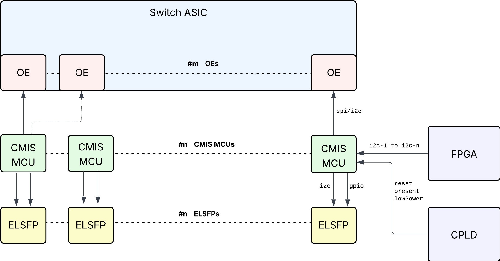
- There shall be an MCU that implements the CMIS interface and abstracts the functioning of the Optical Engine and Pluggable Laser Source from the software.
- This may be a physical MCU (WL) or a virtual MCU.
- One MCU shall not support more than the maximum number of lanes supported by CMIS.
- There shall be a 1:1 mapping between an MCU and an ELSFP, as the software models the MCU as one pluggable device supporting one I2C interface from the ELSFP and its corresponding GPIO pins.
- As long as the data plane is powered on, the software shall be able to communicate with the MCU and program and monitor the OE and ELSFP constantly, except when the MCU is undergoing a Firmware Upgrade.
- Different ELSFPs and/or different OE shall be transparent to the software, from the programming model aspect, except for tuning parameters.
Optical Engine
- The OE should be capable of generating and checking PRBS on the optical line side.
- The OE should be capable of generating and checking PRBS on the electrical system side.
I2C
- Each MCU shall have a dedicated, non-shared I2C bus from the FPGA, supporting a minimum bus speed of 1 MHz.
GPIO
- The MCU (physical or virtual) shall expose the following pins to the CPLD/FPGA:
- Reset:
- A single reset pin that controls the reset of MCU, OE and ELSFP, regardless of their state.
- Resetting should bring the MCU, OE and ELSFP into a clean state as if just after power-on.
- Module Present:
- This pin should indicate the presence of the corresponding ELSFP.
- Low Power:
- This pin should enable and clear low power mode on both the OE and the ELSFP.
- Reset:
LEDs
- There shall be a tri-color (red, yellow, blue) front panel LED per front panel fiber port.
- The LEDs will be driven by FBOSS software through the FPGA/CPLD.
FBOSS Software Requirements
I2C and GPIO access
The BSP shall expose the same interfaces to software as it does for the pluggable optics. For example:
/run/devmap/xcvrs/xcvr_io_1/run/devmap/xcvrs/xcvr_ctrl_1/xcvr_reset_1/run/devmap/xcvrs/xcvr_ctrl_1/xcvr_present_1
For the complete and most recent BSP specification, refer to https://facebook.github.io/fboss/docs/platform/bsp_api_specification/
Software will communicate with the CMIS MCU over I2C using linux standard ioctl calls to
/run/devmap/xcvrs/xcvr_io_X.
CMIS
- The MCU shall support CMIS 5.3 or newer.
- A single MCU shall not support more than the maximum lanes defined by CMIS.
- For example, CMIS 5.3 supports core management features on 4 x 8 lanes.
Datapath Programming
- Software shall only communicate with the CMIS MCU for reading, programming and monitoring. Any internal calibration or communication between OE and ELSFP shall be orchestrated by the CMIS MCU firmware and transparent from FBOSS software.
- The time needed to finish the internal calibration shall be within the advertised time for datapath initialization defined in byte 144 in page 01h in CMIS 5.3.
- The MCU firmware shall implement the CMIS standard Module State Machine and Datapath State Machine, exposing the same control registers for datapath programming as a standard pluggable transceiver.
- All ports on the switch shall be independently and simultaneously programmable.
- The cumulative time for completing datapath programming and achieving link up for all ports on the switch shall be less than 10 seconds.
ASIC and Optical Engine Dependency
- ASIC firmware and CMIS MCU firmware shall be completely separate and upgradable independently.
Features
Firmware Upgrade
- Software will use the CMIS MCU to upgrade firmware for various components (CMIS MCU, OE, and ELSFP) via standard CDB procedures.
- The cumulative time for firmware upgrade of all components - including all MCUs, all OEs and all ELSFPs - should be between 5 minutes (SD) and 10 minutes (MH).
- If the firmware upgrade for CMIS MCU or OE is interrupted, the component shall recover itself with the old firmware automatically after a reset.
ELSFP Monitoring
- The CMIS MCU shall be able to read all diagnostics from the ELSFP as if it were reading the same diagnostics from a pluggable optic.
- The CMIS MCU shall mirror ELSFP diagnostics into the corresponding DOM offsets in the standard upper pages defined in CMIS.
- In addition, the CMIS MCU shall memory-map the ELSFP EEPROM in the reserved upper pages on bank 0. Ideally, the contents of the monitors in the ELSFP pages and the standard upper pages should match, but any differences will be used for debugging purposes.
- The CMIS MCU shall expose read-only access to the ELSFP pages in the above reserved upper pages.